Backed by proven expertise in semiconductor materials, LCY recognizes the pivotal role each cleaning step in advanced packaging plays in yield and chip reliability. Building on this insight, LCY has developed a comprehensive portfolio of wet processing chemicals spanning FEOL, BEOL, and advanced packaging. Powered by proprietary technologies, LCY's solutions deliver unparalleled cleaning performance, high selectivity, and exceptional interface compatibility.
LCY Advanced Wet Chemical Formulation Engineered for Superior Performance
Optimized Efficiency with Low-VOCs for Advanced Processes
LCY Advanced Formulations delivers powerful cleaning performance, high selectivity, and excellent interface compatibility for both etching and cleaning applications in semiconductor manufacturing.
The portfolio enables the selective and thorough removal of residues from laser debonding, temporary bonding/debonding (TBDB), and RIE/ashing processes. It is designed to protect wafers, micro-bumps, and critical metal layers while delivering the surface cleanliness and structural integrity required for advanced packaging.
Featuring a highly controlled etch rate and high selectivity, the formulations minimize undercut while delivering residue-free surfaces that enable reliable downstream processing. They are designed for advanced packaging applications, including wafer-level packaging (WLP), panel-level packaging (PLP), and 2.5D/3D IC integration.

Key Features in Advanced Packaging
- Polysiloxane
- PMMA
- PET
- Epoxy
- Polyimide
- GaAs wafer
- Silicon wafer
- Stainless steel
- Glass substrate
- Non-NMP
- Non-TMAH
- Non-DMSO
Formulated Cleaning Solutions
1. Advanced packaging
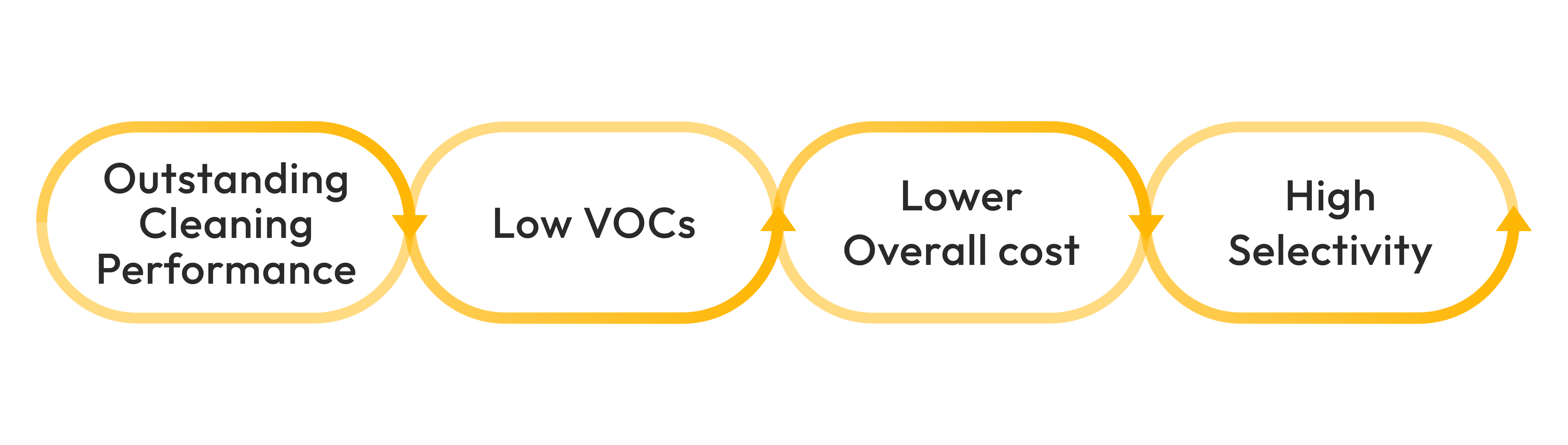
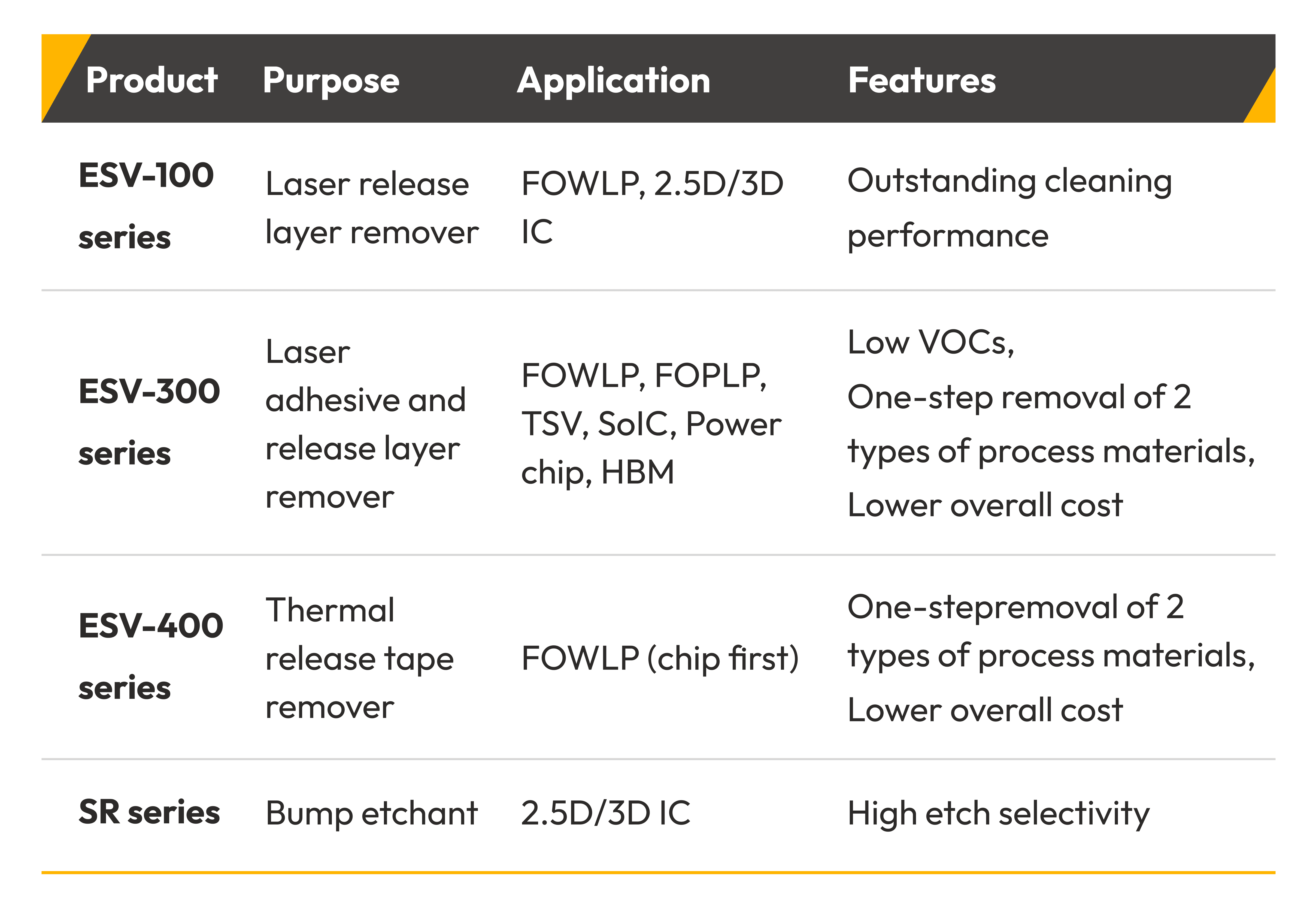
Engineered for advanced packaging, the ESV Series delivers robust cleaning performance with excellent interface protection, meeting the demands of complex processes such as TBDB and laser debonding. It is compatible with WLP, PLP, and 2.5D/3D IC architectures. When combined with the SR Series bump etchants, the portfolio provides a comprehensive wet-processing solution that supports the performance and reliability of next-generation high-performance chips.
TBDB removal
- ESV-100 Series
- ESV-300 Series
- ESV-400 Series
Bump etchant
- SR Series
2. FEOL
The LMG Series offers high-selectivity etching, precisely removing target residues without damaging the underlying substrate. It optimizes downstream processes by ensuring a stable, consistent interface quality in the early stages of wafer processing.
Selective etchant
- LMG Series
3. BEOL
Following RIE, ashing, or bulk PR processing, the LTW and LMG Series rapidly remove stubborn residues while preserving the integrity of metal and dielectric layers. This ensures a seamless transition to subsequent advanced packaging processes. Bulk PR and Post RIE/Ash residue removal
- LTW Series
- LMG Series
Integrated Cross-Process Applications
Powered by material innovation and process expertise, LCY delivers wet processing solutions that set new standards for efficiency, reliability, and sustainability in advanced packaging. By partnering closely with leading semiconductor manufacturers worldwide, LCY is shaping the next generation of processes—faster, more precise, and built for a more sustainable future.
Product Specifications
| Grade | Product Line | Product Type | Application Keywords | |
|---|---|---|---|---|
| ESV | Cleaner | TBDB Removal | Wet chemicals, wet cleaner, debonding cleaner, TBDB remover, adhesive layer removal, release layer removal, residue remover, laser debonding residue cleaning, removal of bonding residue in advanced semiconductor packaging processes and heterogeneous integration processes such as FOWLP, FOPLP, TSV, CoWoS, power chips, and HBM | Ask for sampleFiles download |
| IBC | Cleaner | Flux Cleaner | Wet chemicals, wet cleaner, flux remover, flux cleaner, defluxing agent, solder residue remover, removal of bonding residue in advanced packaging and heterogeneous integration processes, including FOWLP, FOPLP, TSV, SoIC, power chips, and HBM | Ask for sampleFiles download |
| LTW | Cleaner | Ash Residue Removal | Wet chemicals, Wet cleaner, Photoresist stripper, PR stripper, and Post-etch residue remover | Ask for sampleFiles download |
| SR | Etchant | Bump Etchant | Etch micro-bumps in Fan-Out, 2.5D, and 3D ICs to control their dimensions and ensure precise stacked interconnects. | Ask for sampleFiles download |
| LMG | Etchant | Selective Etchant | Polysilicon etchant and Poly-Si etchant | Ask for sampleFiles download |
Frequently Asked Questions
Our process parameters are relatively unique. How do you ensure the cleaners you develop can accurately meet our requirements?
We are not merely selling chemicals; we co-develop process solutions with you. By treating your process parameters as core variables in our R&D, we ensure that the final cleaner delivered not only meets specifications but also enhances your yield and throughput.
Does the product purity meet semiconductor requirements?
We are not just a chemical supplier. We possess comprehensive electronic-grade control capabilities from R&D and precision analysis to mass production. Our goal is to push impurity control to the extreme, allowing customers to develop advanced packaging processes without concerns regarding chemical stability.
What are the differences between these materials and general-purpose chemicals?
Compared with general-purpose chemicals, this product series is specifically designed for semiconductor and advanced packaging processes, with emphasis on process compatibility, material selectivity, and stability.
Through formulation design and quality control, the products effectively reduce potential impact on metals, dielectric layers, packaging structures, or fine patterns, while supporting the cleanliness and consistency required by high-end processes.
Are these products suitable for advanced nodes or advanced packaging processes?
This product series supports the process requirements of advanced nodes and advanced packaging, including high-density interconnects, fine structures, and thin-wafer applications.
Actual applicability still depends on the customer’s process conditions, material combinations, equipment configuration, and quality requirements to ensure stability and reliability in specific processes.
How does the Bump Etchant product perform in controlling undercut? How do you maintain consistent etch rates?
Through highly optimized selectivity and metal-ion control technology, we help customers maintain excellent structural strength and process yield while pursuing ultra-fine pitch.
In the TBDB process, how does your cleaning solution handle high-viscosity adhesive residues?
We redefine high-efficiency cleaning: without compromising environmental or workplace safety, we combine high-viscosity residue removal efficiency with low VOC emissions through precise molecular design, providing a greener and more stable option for your advanced packaging processes.
For Flux cleaner in fine-pitch structures, how does your product address incomplete cleaning caused by capillary effects?
Facing fine-pitch challenges, our Flux Clean solution essentially combines “physical fluid performance” with “chemical dissolution capability.” By reducing surface tension and enhancing molecular-level displacement efficiency, we ensure zero-residue cleaning even in the densest packaging structures.
Do these products comply with sustainability and high-concern substance requirements?
These products incorporate sustainability and supply chain management considerations from the design and development stages. The formulations do not use PFAS, DMSO, NMP, or other highly regulated or restricted substances.
They also balance process performance, operational safety, and environmental friendliness, helping customers meet ESG goals and the industry’s expectations for sustainable manufacturing.


